
Compute & Silicon
The Memory Wall: Why Bandwidth Often Matters More Than Raw Speed
AI chips can often compute far faster than they can fetch data. This gap, known as the memory wall, shapes chip design more than most headlines suggest.

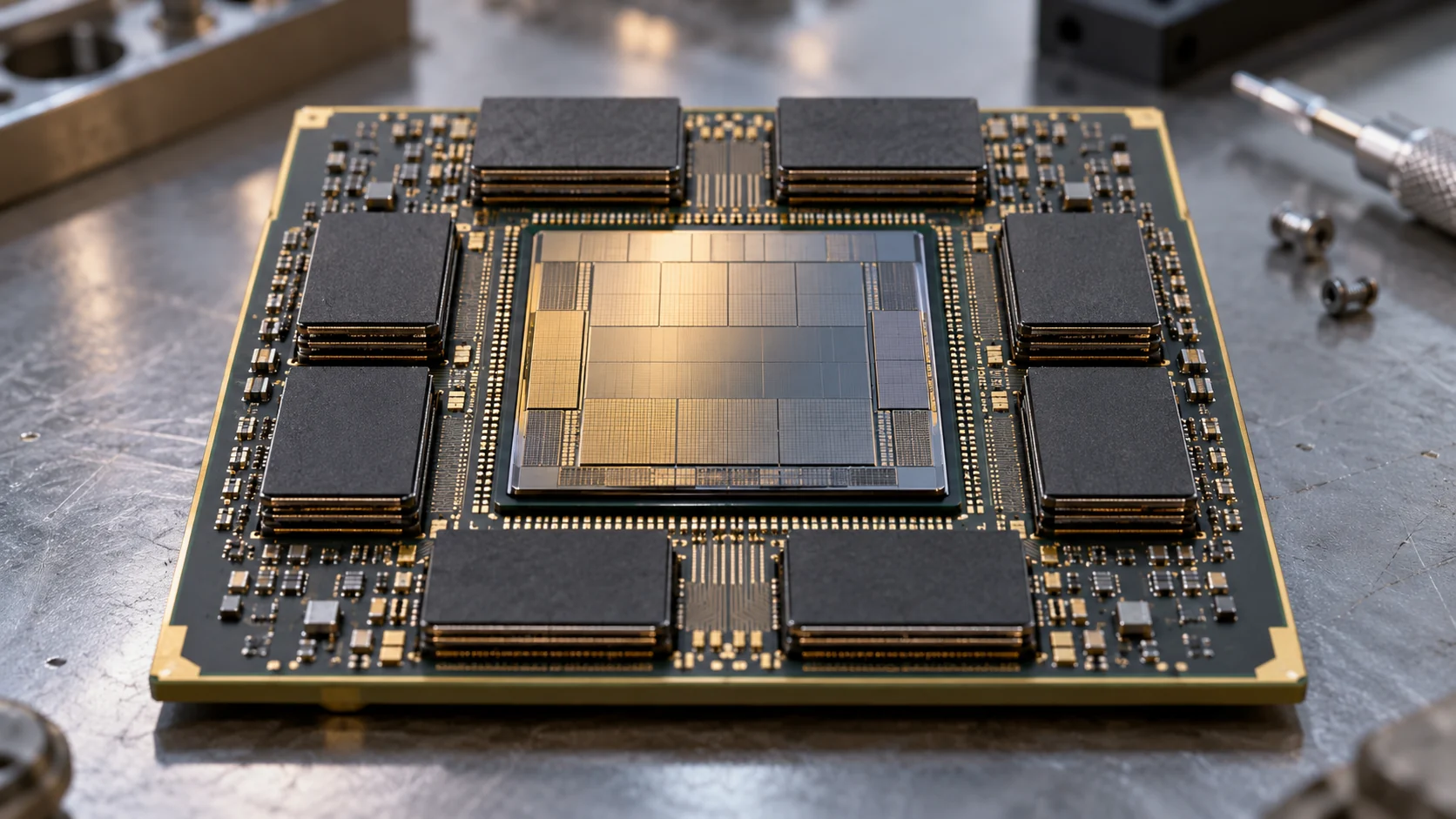
Headline specifications for AI chips usually lead with computing power. Engineers often care just as much about a less glamorous number: how fast the chip can move data in and out of memory. The gap between those two capabilities has a name, the memory wall.
A kitchen analogy
Imagine a restaurant with a superb team of cooks but a single narrow door to the pantry. No matter how skilled the cooks are, they can only work as fast as ingredients come through that door. Add more cooks and the line at the door just gets longer.
In a chip, the math units are the cooks and memory bandwidth is the door. If data cannot arrive fast enough, expensive computing hardware sits idle.
How the wall formed
For decades, processor speed improved faster than memory speed. Engineers noticed this widening gap as far back as the 1990s and coined the term memory wall to describe it. Caches, small pools of very fast memory on the chip, helped bridge the gap for many workloads by keeping frequently used data close at hand.
AI workloads strain that approach. Large models have far more parameters than fit in on-chip cache, so the chip must continually stream numbers from external memory.
Arithmetic intensity
Engineers use a concept called arithmetic intensity to think about this. It measures how many calculations a workload performs for each byte of data it moves.
- High intensity work does lots of math on each piece of data, so the chip is limited by compute.
- Low intensity work does little math per byte, so the chip is limited by memory bandwidth.
Training with large batches of data tends to have higher intensity. Many inference tasks, especially generating text one piece at a time for a single user, tend to have lower intensity. In those cases, memory bandwidth can be the main factor in how quickly answers arrive.
How the industry is responding
Much of the innovation in AI hardware targets the memory wall directly:
- High-bandwidth memory stacks placed right beside the processor.
- Larger on-chip memory to keep more data close.
- Advanced packaging that shortens the distance data travels.
- Lower-precision number formats, which shrink data so more of it moves per second.
- Software techniques that reuse data more efficiently before fetching more.
Some experimental designs go further and try to perform computation inside or very near the memory itself, avoiding much of the data movement altogether.
Reading specs with the wall in mind
When comparing chips, a high peak computing number is only part of the story. Memory bandwidth, memory capacity and how well software keeps the math units busy all determine real performance. A chip with slightly less compute but much more bandwidth may outperform a rival on certain jobs.
Moving data also costs energy, often more than the arithmetic itself. That makes the memory wall not just a speed problem but a power problem, which ties it directly to the broader challenge of powering AI data centers.





Compute & Silicon
Custom AI ASICs vs. GPUs
Custom AI ASICs can deliver strong efficiency on a narrow workload, while GPUs remain valuable because their software ecosystem and flexibility absorb uncertainty.

The custom-ASIC-versus-GPU debate is often framed as a contest between a cheaper chip and a more expensive one. That misses the real decision. A GPU is a general-purpose accelerator with a large software ecosystem. An application-specific integrated circuit is a narrower machine designed around a workload, a power target, or a system architecture.
The winner depends on whether the workload is stable enough to justify specialization. Training, inference, recommendation, search, and video pipelines do not stress hardware in exactly the same way. A model that is efficient today can change after a new architecture, quantization method, context length, or customer demand appears.
What the GPU buys
A GPU’s first advantage is optionality. It can run different model families, numerical formats, kernels, and frameworks. It can be reassigned when demand shifts. That matters for a cloud provider serving many customers and for a company whose AI roadmap is still moving.
The second advantage is software. Mature compiler tools, libraries, kernels, orchestration systems, and developer familiarity reduce the risk between purchasing hardware and putting it into production. A GPU’s list price is not the whole cost; neither is an ASIC’s lower unit cost if engineers spend months rewriting software.
The third advantage is scale. GPUs can be linked into standard or proprietary fabrics, with established server, cooling, and support ecosystems. A customer can often rent them before it owns them, which converts a large capital decision into a more flexible operating expense.
The GPU’s weaknesses are also clear. The chip may carry circuitry for workloads the customer does not use. Its memory and network design may be optimized for a broad market rather than one application. High demand can create shortages, and power density can push a facility’s cooling and electrical systems beyond their original design.
What the ASIC buys
A custom ASIC can remove general-purpose features and use the saved area or power for the specific operations that matter. It may deliver more performance per watt, better latency, or lower cost per inference when the workload is predictable.
An ASIC can also be part of a broader system strategy. Google and other hyperscalers have built custom accelerators because owning the silicon roadmap can reduce dependence on a merchant vendor and let the company tune hardware to its software stack. Intel described an expanded 2026 collaboration with Google around custom ASIC-based infrastructure processing units that offload networking, storage, and security functions from host CPUs. That is a reminder that “custom AI silicon” is not limited to a chip that performs matrix multiplication.
The costs appear before production
ASIC design requires architecture, verification, physical design, software, packaging, testing, and manufacturing commitments. A company must pay those costs before it knows how many units it will ship.
The minimum efficient volume can be high. If a custom chip saves $1,000 per accelerator but costs $300 million to develop and qualify, the business needs more than 300,000 units before ignoring financing, support, and inventory risk. If the workload changes before that volume is reached, the savings may disappear.
Advanced packaging and high-bandwidth memory can add another constraint. Micron reported in March 2025 that its HBM output for calendar 2025 was sold out and that it was already discussing 2026 demand with customers. A custom ASIC that cannot secure memory, substrates, and packaging is not a complete product.
A practical comparison must use system metrics
Compare the two options at the system level. Measure useful work per rack, tokens per second per watt, cost per million tokens, time to train, memory capacity, software migration effort, and failure-recovery behavior.
Do not compare a peak chip number from a data sheet with a measured production result from another platform. Ask whether the benchmark uses the same model, batch size, sequence length, precision, compiler version, and utilization target.
A GPU may win on time to market even if an ASIC wins on energy. The value of six months of earlier service can be material for a cloud provider. Conversely, an inference fleet with a stable model and high utilization may benefit from a specialized accelerator.
The market is moving toward heterogeneous systems
The likely outcome is not one winner. General-purpose GPUs will remain useful for training, new models, and workloads with uncertain demand. Custom ASICs will take more of the predictable inference, networking, storage, and recommendation work. CPUs, DPUs, and specialized accelerators will handle other parts of the system.
Intel’s Gaudi 3 product materials emphasize standard Ethernet, open software, and a migration path for customers moving from GPU-based systems. That positioning shows the market’s pressure point: customers want acceleration without locking every layer of the stack to one vendor.
The decision rule is simple. Use GPUs when flexibility, software, and deployment speed are worth paying for. Use an ASIC when the workload is stable, volume is large, memory and packaging are secured, and the organization can support a separate software and operations path.
The best analysis treats silicon as a fleet decision, not a chip-shopping exercise. The question is which architecture produces reliable, adaptable work at the lowest total cost over the period in which the workload is likely to remain stable.
There is also a strategic lock-in cost. A GPU fleet may be portable across cloud providers and model frameworks, while a custom accelerator can require a dedicated compiler, kernel library, scheduler, and support team. That lock-in may be acceptable when demand is large and stable. It is dangerous when the business case assumes a model architecture will remain unchanged for five years. The best ASIC programs preserve a fallback path: compatible APIs, exportable model formats, or enough GPU capacity to absorb new workloads while the specialized stack catches up.
Sources
- Micron, “Fiscal Q2 2025 Investor Materials,” March 20, 2025: investors.micron.com
- TSMC, “2025 Annual Report,” 2026: investor.tsmc.com
- Intel, “Intel Gaudi AI Accelerator Products,” accessed October 2026: intel.com
- Intel, “Intel and Google Deepen Collaboration to Advance AI Infrastructure,” April 9, 2026: newsroom.intel.com
- IEA, “Energy and AI,” April 10, 2025: iea.org
BOSSTOX Research articles are drafted with AI assistance and reviewed by our editors before publication. See our editorial standards.
Compute & Silicon
HBM Is a Bottleneck Because AI Memory Is a Stack, Not a Chip
High-bandwidth memory limits AI accelerator shipments through several linked manufacturing steps, so a strong DRAM market alone does not guarantee enough HBM for the next GPU cycle.
The memory next to the compute
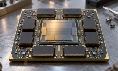
High-bandwidth memory, or HBM, is the memory placed close to an AI accelerator and connected through a wide interface. It is built by stacking DRAM dies vertically and connecting them with through-silicon vias, or TSVs. The package can move data at enormous rates, but it is also harder to manufacture than a conventional memory module.
That is why HBM can become a bottleneck even when the broader DRAM market has available capacity. The constraint may sit in the memory stack, the base die, the TSV process, the packaging line, thermal qualification or the final integration of memory and logic.
The numbers tell the story
On September 26, 2024, SK hynix announced mass production of a 12-layer HBM3E product with 36 gigabytes of capacity. The company said the product reached 9.6 gigabits per second and that each DRAM die had been made 40% thinner to fit twelve layers in the same overall thickness as the prior eight-layer product. SK hynix also said the 12-layer design improved capacity by 50% over its prior 8-layer product.
Micron’s HBM3E materials describe an 8-high, 24-gigabyte product with more than 9.2 gigabits per second data rate and more than 1.2 terabytes per second of bandwidth. Micron said its 12-high, 36-gigabyte version was expected to ramp in early calendar 2025.
These specifications are not interchangeable. An accelerator may be designed around a particular HBM generation, stack height, interface width, thermal envelope and package layout. A memory supplier can have the right capacity but still fail to qualify the exact configuration required by the accelerator program.
Why capacity is hard to add
HBM growth requires more than adding DRAM wafer starts. The manufacturing chain includes:
- DRAM wafer fabrication.
- Thinning and preparing individual dies.
- Testing and binning dies.
- Stacking dies with TSV connections.
- Attaching the stack to a base die or package substrate.
- Thermal and electrical qualification.
- Final integration with the AI accelerator.
Each step has yield risk. If one die in a stack fails, the entire stack may be downgraded or scrapped. Thinner dies can make more layers possible, but they also make warpage, handling and thermal problems more difficult. SK hynix said its advanced mass reflow-molded underfill process helped with warpage control and heat dissipation in the 12-layer HBM3E product.
The packaging connection
HBM is part of the advanced-package bottleneck described in the CoWoS discussion. The memory must be connected to the logic die with short, high-bandwidth paths. The package needs enough interposer area, substrate capacity and test capability. If HBM supply rises but advanced packaging does not, accelerator output can still be constrained.
That is why the right question is not “How many HBM wafers can a company make?” It is “How many qualified, packaged HBM stacks can reach the accelerator assembly line at the required yield and date?”
Qualification creates another delay. AI customers need to validate signal integrity, error rates, thermals, power draw and reliability at a system level. A new HBM stack may look attractive on a product sheet but still require months of testing before it can ship into a production accelerator.
What buyers should watch
AI infrastructure buyers should track HBM by generation and configuration. A purchase plan should identify capacity per stack, number of stacks per accelerator, bandwidth, supplier and expected qualification date. It should also show whether the product is already in volume production or merely sampled.
Investors should watch supplier commentary for mix, not just revenue. A memory company can report strong HBM sales while still changing the product mix from 8-high to 12-high or from HBM3E to HBM4. Higher-value stacks may increase revenue per package but also consume more dies and advanced assembly steps.
The market signal is customer qualification. A supplier’s announcement of a development milestone is useful. A production shipment to a named accelerator program is stronger. A disclosed multi-year supply agreement may be stronger still, although it does not guarantee that the final system will sell at the forecast volume.
BOSSTOX takeaway
HBM is a systems bottleneck. It connects memory-fab capacity, die yield, stacking technology, thermal engineering, packaging and customer qualification. The bottleneck can move from one step to another as suppliers expand.
For AI infrastructure analysis, report HBM with the same discipline used for GPUs: generation, stack height, capacity, bandwidth, qualification status, production date and package destination. “HBM demand is strong” is a market statement. “36GB 12-layer HBM3E entered mass production on September 26, 2024” is an auditable operating fact.
The memory bottleneck also affects the economics of each accelerator. More HBM can improve throughput, but it adds memory cost, package area and thermal load. If a model is bandwidth-bound, the extra memory may deliver a real performance gain. If it is compute-bound or poorly optimized, the same memory may not improve utilization enough to justify the premium. Data-center buyers should therefore connect HBM configuration to workload benchmarks rather than compare capacity alone.
There is a timing problem as well. A new HBM generation can be announced before the complete accelerator platform is qualified. The deployment schedule must wait for the slowest item: memory production, package assembly, system validation or software readiness. That is why a memory announcement can be strategically important without changing near-term server availability.
For capacity planning, a buyer should map the HBM requirement per server and per rack. If one accelerator uses six stacks and a rack contains 72 accelerators, the rack requires 432 stacks before spares. A 10,000-accelerator deployment would require 60,000 stacks. The arithmetic does not predict supply, but it shows why a small change in stack count or yield can move a large project’s schedule.
HBM also carries a qualification cost. A vendor may need to validate a new stack with the full accelerator, board, firmware and cooling system. The customer may accept a faster product only after testing reliability under sustained load. That makes customer sampling an important milestone, but not the same as high-volume availability.
One more practical issue is inventory policy. Because HBM is expensive and sensitive to configuration, a buyer may not be able to substitute one supplier’s stack for another at the last minute. The system bill of materials, firmware and validation plan must preserve that option before a shortage appears. A project that waits until a missed shipment to qualify a second source may lose an entire deployment window.
Sources
- SK hynix, “Begins Volume Production of the World’s First 12-Layer HBM3E,” September 26, 2024: news.skhynix.com
- SK hynix, “The World’s Largest Capacity 16-Layer HBM3E Under Development,” November 2024: news.skhynix.com
- Micron, “HBM3E Product Brief”: assets.micron.com
- TSMC 2024 Annual Report, 3DFabric and CoWoS: investor.tsmc.com
BOSSTOX Research articles are drafted with AI assistance and reviewed by our editors before publication. See our editorial standards.
Compute & Silicon
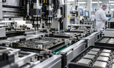
GPU Supply Chains: How AI Hardware Gets Made, Moved, and Bottlenecked
An AI accelerator is the end of a long industrial chain. The slowest link — not the headline chip — usually sets the delivery date.
Key points
- Leading-edge fabrication, advanced packaging and high-bandwidth memory are three separate bottlenecks.
- Rack-scale systems integrate compute, networking, power and cooling, which also makes their supply chains more interdependent.
- A purchase order for GPUs is not the same as guaranteed, usable capacity.
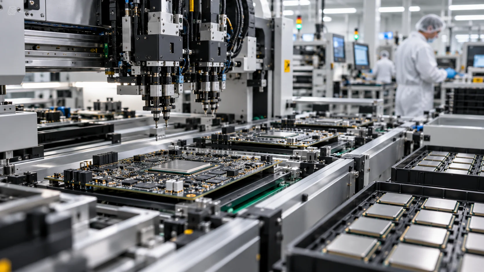
The public conversation about AI hardware often starts and ends with the name of a GPU. The real supply chain is much longer. A modern accelerator depends on chip design, leading-edge wafer fabrication, advanced packaging, high-bandwidth memory, substrates, networking, power systems, servers, and data-center installation. A shortage at any one point can delay the whole system.
A GPU is not simply a faster version of a desktop graphics card. AI accelerators are built around parallel operations and large memory systems. Training and inference move enormous amounts of data between processors and memory. That makes bandwidth, packaging, and interconnects as important as raw arithmetic performance.
Bottleneck one: leading-edge fabrication
The first bottleneck is advanced manufacturing. Leading AI chips use sophisticated process technology and must be produced with extremely high yields. A design may work in the laboratory and still be difficult to manufacture at volume. Each wafer contains many dies, and small defects can reduce the number of usable chips. As designs get larger, the economics of yield become more complicated.
Bottleneck two: advanced packaging
Advanced packaging is the next constraint. A high-end AI accelerator may combine multiple compute dies with high-bandwidth memory in one package. This is valuable because it shortens the path between compute and memory, but it requires specialized equipment and process control. Packaging capacity cannot always be expanded as quickly as demand for finished systems.
Bottleneck three: memory
Memory is a separate supply-chain problem. AI workloads use high-bandwidth memory to feed accelerators fast enough. If accelerator production rises faster than memory packaging capacity, a chip company can have working silicon but still lack complete products. Memory markets also respond to demand from phones, servers, and other electronics, so AI does not operate in isolation.
Everything else in the rack
Then there are substrates, interposers, circuit boards, power supplies, and networking components. A data-center rack needs more than GPUs. It needs CPUs, storage, switches, cables, transceivers, firmware, racks, and cooling equipment. The component with the longest lead time can set the delivery date for the entire system.
Modern AI systems add another layer: scale-up and scale-out networking. Inside a rack, accelerators need very fast links to exchange model data. Across racks, clusters need a fabric that can coordinate thousands of devices. NVIDIA describes its Blackwell systems as rack-scale designs in which GPUs, CPUs, memory, networking, power, and cooling are engineered together. That integration improves performance, but it also makes the supply chain more interdependent.
Geopolitics and policy
Geopolitics matters because the supply chain crosses borders. Chip design may happen in one country, wafer fabrication in another, packaging in a third, and final system assembly somewhere else. Export controls can change which products can be sold into a market. Subsidies can influence where factories are built. Natural disasters, shipping interruptions, energy shortages, and workforce constraints can all create delays.
The CHIPS for America program is one government response. The U.S. Department of Commerce describes the program as a combination of manufacturing incentives and research support intended to expand domestic semiconductor capacity. That does not mean every part of the AI supply chain will move to one country. It does mean policymakers are trying to reduce reliance on a narrow set of facilities and regions.
What buyers should ask
For buyers, the lesson is to think in systems and time horizons. A purchase order for GPUs is not the same as guaranteed capacity. Buyers should ask which exact model, memory configuration, server platform, networking fabric, and support contract are included. They should also ask how long replacement parts will remain available and whether the system can use more than one accelerator generation.
Cloud providers face the same issue at larger scale. They can negotiate supply, reserve capacity, and design multiple platform options. Smaller businesses usually cannot. They may be better served by buying access to a managed service rather than trying to own the entire hardware stack.
The supply chain will improve, but demand will also keep changing. A new model architecture can shift demand from one type of accelerator to another. Better software can reduce the hardware required for a given task. A shortage today may become an oversupply later if a product is difficult to repurpose.
AI hardware is therefore best understood as an industrial system. The winning infrastructure strategy is not simply to acquire the most powerful chip. It is to secure a reliable combination of compute, memory, networking, power, cooling, software, service, and replacement capacity.
What BOSSTOX is watching
- Packaging capacity additions relative to wafer capacity.
- High-bandwidth memory allocation between AI and other electronics.
- How long each accelerator generation stays supported with spare parts.
Sources
- NVIDIA, Blackwell Architecture
- NVIDIA, Data Center Architecture
- U.S. Department of Commerce, CHIPS for America funding
- TSMC, U.S. investment announcement
BOSSTOX Research articles are drafted with AI assistance and reviewed by our editors before publication. See our editorial standards.

The BOSSTOX App: Markets and the AI Build-Out on iPhone, iPad and Apple Watch

AI Server Rack Power Density, 2024-2027
The Life Cycle of a Data Center: Buildings Last Decades, Servers Do Not

Custom AI ASICs vs. GPUs

Gas Turbines on Data-Center Campuses

Transformer Lead Times Are Becoming a Data-Center Schedule Risk

GPU Supply Chains: How AI Hardware Gets Made, Moved, and Bottlenecked

Battery Storage at AI Sites
The BOSSTOX App: Markets and the AI Build-Out on iPhone, iPad and Apple Watch
AI Server Rack Power Density, 2024-2027
The Life Cycle of a Data Center: Buildings Last Decades, Servers Do Not
Custom AI ASICs vs. GPUs
-
 Power & Grid2 weeks ago
Gas Turbines on Data-Center Campuses
-
 Power & Grid2 weeks ago
Transformer Lead Times Are Becoming a Data-Center Schedule Risk
-
 Compute & Silicon3 weeks ago
GPU Supply Chains: How AI Hardware Gets Made, Moved, and Bottlenecked
-
 Power & Grid2 weeks ago
Battery Storage at AI Sites
-

 Cooling4 weeks ago
Water Use and Dry Coolers: The Tradeoff AI Sites Cannot Avoid
-

 Explainers1 month ago
Explainer: What an AI Inference Stack Actually Does
-

 Explainers1 month ago
AI Costs for Small Businesses: A Practical Model Before You Buy GPUs
-
 Compute & Silicon3 weeks ago
HBM Is a Bottleneck Because AI Memory Is a Stack, Not a Chip